- 您现在的位置:买卖IC网 > Sheet目录3893 > PIC16F723A-I/SS (Microchip Technology)MCU PIC 7KB FLASH XLP 28-SSOP
PIC16(L)F722A/723A
DS41417B-page 124
2010-2012 Microchip Technology Inc.
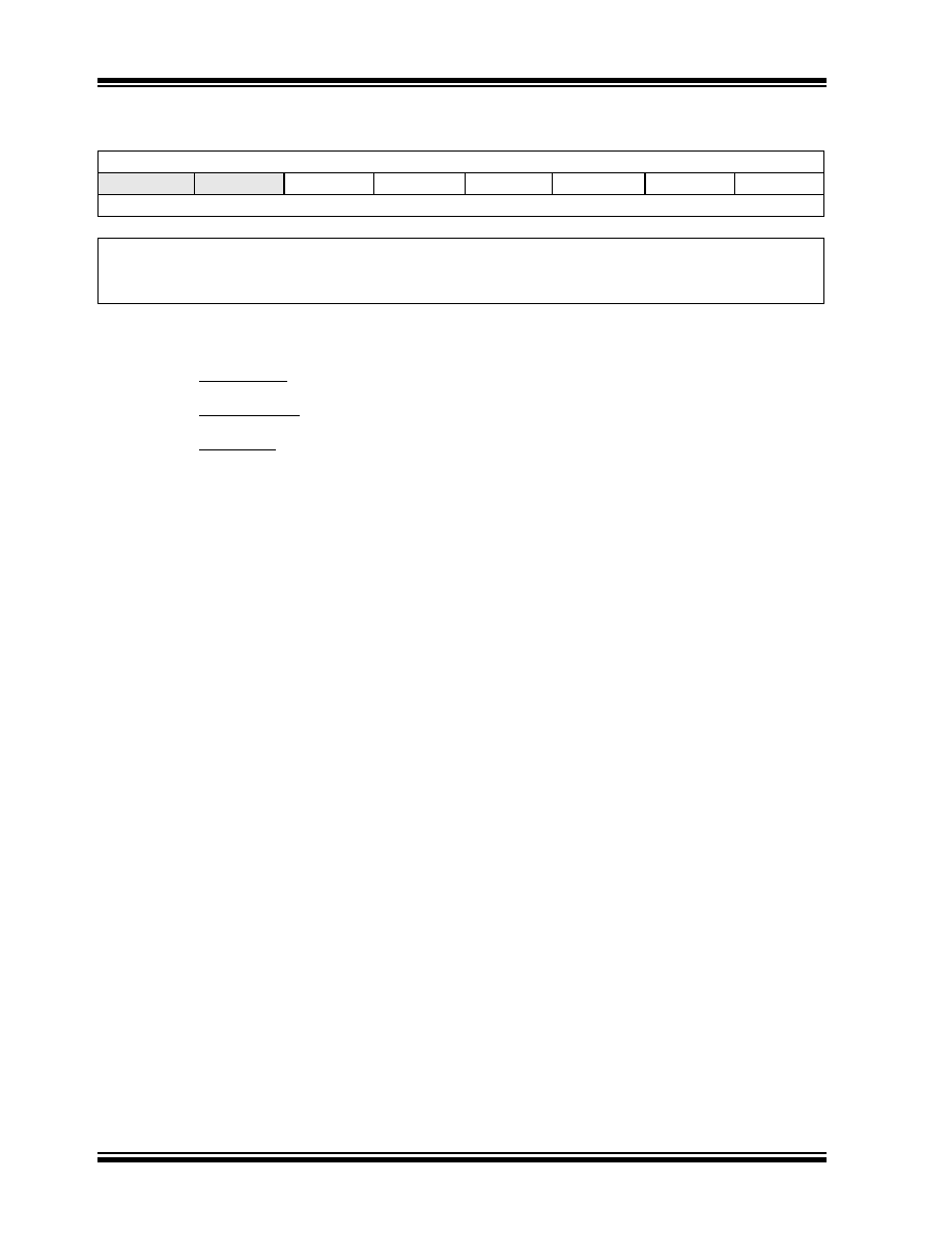
REGISTER 15-1:
CCPxCON: CCPx CONTROL REGISTER
U-0
R/W-0
—
DCxB1
DCxB0
CCPxM3
CCPxM2
CCPxM1
CCPxM0
bit 7
bit 0
Legend:
R = Readable bit
W = Writable bit
U = Unimplemented bit, read as ‘0’
-n = Value at POR
‘1’ = Bit is set
‘0’ = Bit is cleared
x = Bit is unknown
bit 7-6
Unimplemented: Read as ‘0’
bit 5-4
DCxB<1:0>: PWM Duty Cycle Least Significant bits
Capture mode:
Unused
Compare mode:
Unused
PWM mode:
These bits are the two LSbs of the PWM duty cycle. The eight MSbs are found in CCPRxL.
bit 3-0
CCPxM<3:0>: CCP Mode Select bits
0000 = Capture/Compare/PWM off (resets CCP module)
0001 = Unused (reserved)
0010 = Compare mode, toggle output on match (CCPxIF bit of the PIRx register is set)
0011 = Unused (reserved)
0100 = Capture mode, every falling edge
0101 = Capture mode, every rising edge
0110 = Capture mode, every 4th rising edge
0111 = Capture mode, every 16th rising edge
1000 = Compare mode, set output on match (CCPxIF bit of the PIRx register is set)
1001 = Compare mode, clear output on match (CCPxIF bit of the PIRx register is set)
1010 = Compare mode, generate software interrupt on match (CCPxIF bit is set of the PIRx register,
CCPx pin is unaffected)
1011 = Compare mode, trigger special event (CCPxIF bit of the PIRx register is set, TMR1 is reset
and A/D conversion(1) is started if the ADC module is enabled. CCPx pin is unaffected.)
11xx = PWM mode.
Note 1: A/D conversion start feature is available only on CCP2.
发布紧急采购,3分钟左右您将得到回复。
相关PDF资料
PIC12C508A-04/SN
IC MCU OTP 512X12 8SOIC
PIC12C509A-04/SM
IC MCU OTP 1KX12 8-SOIJ
PIC16LF627T-04I/SO
IC MCU FLASH 1KX14 COMP 18SOIC
PIC12C509A-04/P
IC MCU OTP 1KX12 8DIP
PIC18LC452T-I/PT
IC MCU OTP 16KX16 A/D 44TQFP
PIC12LF1822-I/MF
IC MCU 8BIT FLASH 8DFN
PIC12F1822-I/P
IC MCU 8BIT FLASH 8PDIP
PIC12F1822-I/MF
IC MCU 8BIT FLASH 8DFN
相关代理商/技术参数
PIC16F723AT-I/ML
功能描述:8位微控制器 -MCU 7KB Flash 1.8V-5.5V. 16 MHz int Osc RoHS:否 制造商:Silicon Labs 核心:8051 处理器系列:C8051F39x 数据总线宽度:8 bit 最大时钟频率:50 MHz 程序存储器大小:16 KB 数据 RAM 大小:1 KB 片上 ADC:Yes 工作电源电压:1.8 V to 3.6 V 工作温度范围:- 40 C to + 105 C 封装 / 箱体:QFN-20 安装风格:SMD/SMT
PIC16F723AT-I/MV
功能描述:8位微控制器 -MCU 7KB Flash 1.8V-5.5V. 16 MHz int Osc RoHS:否 制造商:Silicon Labs 核心:8051 处理器系列:C8051F39x 数据总线宽度:8 bit 最大时钟频率:50 MHz 程序存储器大小:16 KB 数据 RAM 大小:1 KB 片上 ADC:Yes 工作电源电压:1.8 V to 3.6 V 工作温度范围:- 40 C to + 105 C 封装 / 箱体:QFN-20 安装风格:SMD/SMT
PIC16F723AT-I/SO
功能描述:8位微控制器 -MCU 7KB Flash 1.8V-5.5V. 16 MHz int Osc RoHS:否 制造商:Silicon Labs 核心:8051 处理器系列:C8051F39x 数据总线宽度:8 bit 最大时钟频率:50 MHz 程序存储器大小:16 KB 数据 RAM 大小:1 KB 片上 ADC:Yes 工作电源电压:1.8 V to 3.6 V 工作温度范围:- 40 C to + 105 C 封装 / 箱体:QFN-20 安装风格:SMD/SMT
PIC16F723AT-I/SS
功能描述:8位微控制器 -MCU 7KB Flash 1.8V-5.5V. 16 MHz int Osc RoHS:否 制造商:Silicon Labs 核心:8051 处理器系列:C8051F39x 数据总线宽度:8 bit 最大时钟频率:50 MHz 程序存储器大小:16 KB 数据 RAM 大小:1 KB 片上 ADC:Yes 工作电源电压:1.8 V to 3.6 V 工作温度范围:- 40 C to + 105 C 封装 / 箱体:QFN-20 安装风格:SMD/SMT
PIC16F723-E/ML
功能描述:8位微控制器 -MCU 7 KB Flash 18V-55V 16 MHz Int Osc RoHS:否 制造商:Silicon Labs 核心:8051 处理器系列:C8051F39x 数据总线宽度:8 bit 最大时钟频率:50 MHz 程序存储器大小:16 KB 数据 RAM 大小:1 KB 片上 ADC:Yes 工作电源电压:1.8 V to 3.6 V 工作温度范围:- 40 C to + 105 C 封装 / 箱体:QFN-20 安装风格:SMD/SMT
PIC16F723-E/MV
功能描述:8位微控制器 -MCU 7KB Flash 1.8V-5.5V RoHS:否 制造商:Silicon Labs 核心:8051 处理器系列:C8051F39x 数据总线宽度:8 bit 最大时钟频率:50 MHz 程序存储器大小:16 KB 数据 RAM 大小:1 KB 片上 ADC:Yes 工作电源电压:1.8 V to 3.6 V 工作温度范围:- 40 C to + 105 C 封装 / 箱体:QFN-20 安装风格:SMD/SMT
PIC16F723-E/SO
功能描述:8位微控制器 -MCU 7 KB Flash 18V-55V 16 MHz Int Osc RoHS:否 制造商:Silicon Labs 核心:8051 处理器系列:C8051F39x 数据总线宽度:8 bit 最大时钟频率:50 MHz 程序存储器大小:16 KB 数据 RAM 大小:1 KB 片上 ADC:Yes 工作电源电压:1.8 V to 3.6 V 工作温度范围:- 40 C to + 105 C 封装 / 箱体:QFN-20 安装风格:SMD/SMT
PIC16F723-E/SP
功能描述:8位微控制器 -MCU 7 KB Flash 18V-55V 16 MHz Int Osc RoHS:否 制造商:Silicon Labs 核心:8051 处理器系列:C8051F39x 数据总线宽度:8 bit 最大时钟频率:50 MHz 程序存储器大小:16 KB 数据 RAM 大小:1 KB 片上 ADC:Yes 工作电源电压:1.8 V to 3.6 V 工作温度范围:- 40 C to + 105 C 封装 / 箱体:QFN-20 安装风格:SMD/SMT